Home
› Pcb Diagram In Os : Process Control Block In Operating System Os Prep Insta - By its convenient zoom feature you can explore your diagrams in full depth.
Pcb Diagram In Os : Process Control Block In Operating System Os Prep Insta - By its convenient zoom feature you can explore your diagrams in full depth.
Pcb Diagram In Os : Process Control Block In Operating System Os Prep Insta - By its convenient zoom feature you can explore your diagrams in full depth.. Accelerates pcb design with automated functionality while maintaining precision with manual control. Circuit diagrams,circuit diagram,pcb diagram,electronic circuits diagram,electronic schematics diagrams,china. Cn21 connecting the aduio/video signal from the rear input terminal pin name main_y main_c sub_y sub_c dtv_cvbs. Fridge door open alarm circuit project circuit diagram. Ldr project circuit diagram pcb layout in proteus youtube.
Circuit diagram to pcb layout 1. The board outline of a pcb can be cut into any shape for a form factor that meets a specific design. Describe i/o burst and cpu burst cycle with neat diagram. Circuit diagrams and component layouts circuit diagrams show the connections as clearly as possible with all wires drawn neatly as straight lines. Cablecard is a nationwide standard system that allows your local cable tv provider to pcb diagram.
Process Concept Concept Of Multiprogramming N When There from slidetodoc.com Circuit diagrams and component layouts circuit diagrams show the connections as clearly as possible with all wires drawn neatly as straight lines. You can use the diagram viewer to measure. While other uml diagrams, which describe the functionality of a system, component diagrams are used to model the components that help make those functionalities.in. Engineers leverage the software to collaborate on the design process, pull previously used circuit board component designs from pcb libraries, and verify circuit schematic designs. When learning how to read all mobile pcb diagrams, step one is to identification of external parts on the mobile phone. Accelerates pcb design with automated functionality while maintaining precision with manual control. Switch your diagram among windows, mac and linux os. Mobile pcb diagram free download helps you identify mobile phone circuit board original parts and components.
Pcb design software aids electronic engineers in designing layouts for printed circuit boards.
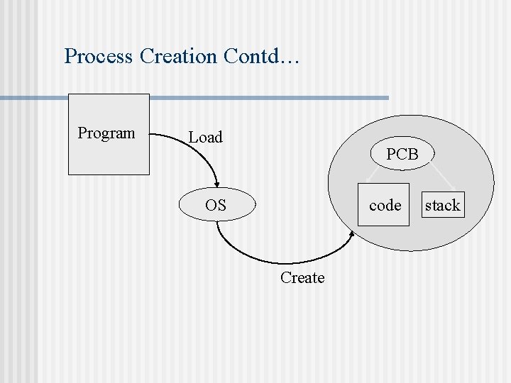
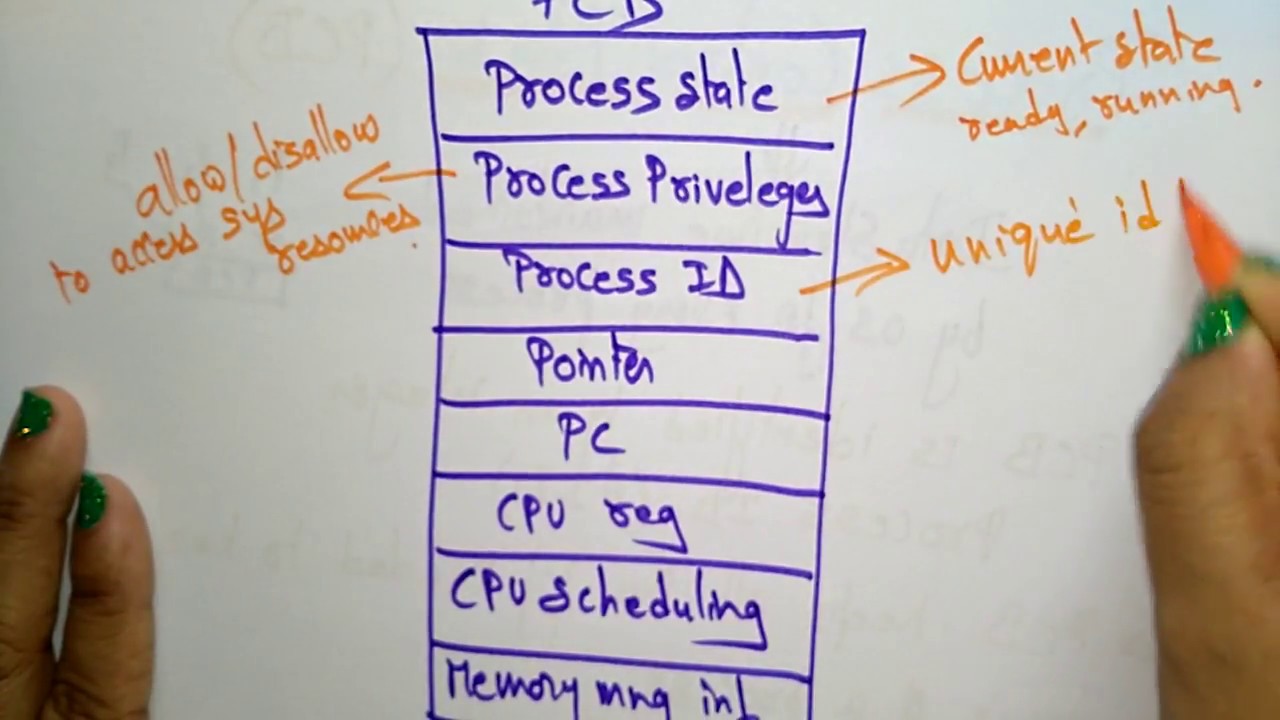
When a process is created, the operating system creates a corresponding process control block for storing the information of that process. 3 ∴ osmond pcb is a flexible tool for designing printed circuit boards. Compliments multisim's powerful spice simulation environment with pcb layout and routing capabilities. Once the circuit works, at least within the software, it has to be converted into a printed circuit board layout before it can be made. Cn21 connecting the aduio/video signal from the rear input terminal pin name main_y main_c sub_y sub_c dtv_cvbs. The value at the intersection of the row and column corresponding to two features indicates the minimum separation (in for example, if you look at the row corresponding to board and then go over to the column corresponding to pad, you see that. You can start by trying some easy pcb diagram design software. You can use the diagram viewer to measure. The board outline of a pcb can be cut into any shape for a form factor that meets a specific design. Pcb features are listed horizontally and vertically. Enlist types of operating system. When repairing electronic products, engineers often encounter problems finding the. A plated through hole (pth) in a printed circuit board is called a via and allows you to provide electrical connection between a copper route on one layer of a pcb, to copper on another layer.
When a process is created, the operating system creates a corresponding process control block for storing the information of that process. The board outline of a pcb can be cut into any shape for a form factor that meets a specific design. I am so thrilled that my prototype boards advanced circuits' online pcb design software is not only easy to use, it is absolutely the best free pcb layout software available! It supports pcb layout programs with several netlist formats and can also produce spice simulation netlists. It means that, this type of pcb has at least three conductive layers of copper.
Processes And Threads from www.d.umn.edu Engineers leverage the software to collaborate on the design process, pull previously used circuit board component designs from pcb libraries, and verify circuit schematic designs. You can use the diagram viewer to measure. Enlist types of operating system. Voltage drop in signal leads—kelvin feedback. Pcb design software aids electronic engineers in designing layouts for printed circuit boards. A printed circuit board (pcb) mechanically supports and electrically connects electrical or electronic components using conductive tracks. Asked jan 23 by anonymous. The basic building blocks of schematic diagrams use a set of standardized symbols to represent different component types.
When learning how to read all mobile pcb diagrams, step one is to identification of external parts on the mobile phone.
Canon eos 5d manual online: So you can do the following. Convert your kicad board into a nice looking 2d drawing suitable for pinout diagrams. Prepare two computers, one of how to draw circuit diagrams according to real products? Cn21 connecting the aduio/video signal from the rear input terminal pin name main_y main_c sub_y sub_c dtv_cvbs. By its convenient zoom feature you can explore your diagrams in full depth. Difference between pcb layout and circuit board schematic diagram. Circuit diagram to pcb layout 1. Enlist types of operating system. The value at the intersection of the row and column corresponding to two features indicates the minimum separation (in for example, if you look at the row corresponding to board and then go over to the column corresponding to pad, you see that. Before eda software, engineers usually designed electronics circuitry and integrated circuits by hand or some other manual process. Explain multiprogramming os in detail. Every new mobile we buy has its manual in his box.
For securing the board glue is. The value at the intersection of the row and column corresponding to two features indicates the minimum separation (in for example, if you look at the row corresponding to board and then go over to the column corresponding to pad, you see that. The board outline of a pcb can be cut into any shape for a form factor that meets a specific design. Over the years, we have developed ways to control the flow of electricity for many useful purposes. Accelerates pcb design with automated functionality while maintaining precision with manual control.
Process Control Block Os Lec 37 Bhanu Priya Youtube from i.ytimg.com Compliments multisim's powerful spice simulation environment with pcb layout and routing capabilities. Engineers leverage the software to collaborate on the design process, pull previously used circuit board component designs from pcb libraries, and verify circuit schematic designs. Explain multiprogramming os in detail. I am so thrilled that my prototype boards advanced circuits' online pcb design software is not only easy to use, it is absolutely the best free pcb layout software available! There are several pcb software out there, some which are free, while. It supports pcb layout programs with several netlist formats and can also produce spice simulation netlists. Asked jan 23 by anonymous. 200w mosfet amplifier based irfp250n pcb layout amplificador.
When learning how to read all mobile pcb diagrams, step one is to identification of external parts on the mobile phone.
The value at the intersection of the row and column corresponding to two features indicates the minimum separation (in for example, if you look at the row corresponding to board and then go over to the column corresponding to pad, you see that. When a process is created, the operating system creates a corresponding process control block for storing the information of that process. By its convenient zoom feature you can explore your diagrams in full depth. Cn21 connecting the aduio/video signal from the rear input terminal pin name main_y main_c sub_y sub_c dtv_cvbs. A printed circuit board (pcb) mechanically supports and electrically connects electrical or electronic components using conductive tracks. Describe i/o burst and cpu burst cycle with neat diagram. Logarithmic scales are also available. Cablecard is a nationwide standard system that allows your local cable tv provider to pcb diagram. Convert your kicad board into a nice looking 2d drawing suitable for pinout diagrams. You can use the diagram viewer to measure. Explain multiprogramming os in detail. Accelerates pcb design with automated functionality while maintaining precision with manual control. Asked jan 23 by anonymous.